This post deals about components
of infrared camera system. Infrared region ranges from 0.7 μm to 1000
μm. For convenience infrared is split into shortwave (3 to 5 μm)
and longwave (8 to 12 μm) bands [1]. Few
types of thermal camera are shown in Figure 1. Their appearance will be similar
to conventional cameras.
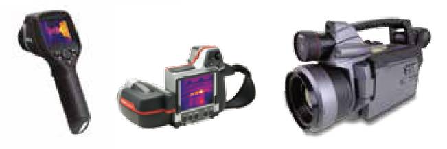 |
| Figure 1. Various types of Thermal Imaging Cameras Courtesy ref. [3] |
In
ambient temperature, radiant flux emitted by is more in longwave than shortwave.
But shortwave is more sensitive to longwave at ambient temperature conditions.
Sun radiation is small but significant in shortwave range. It is helpful to
increase image contrast in some cases and in cases like measuring temperature
of an object, sun radiation is unwanted. Longer wavelength can penetrate mist and
smoke better than shortwave. So longwave always preferred in surveillance
applications.
At
cursory level, architecture of thermal cameras will be similar to conventional
cameras. The main differences are presence of scanning subsystem and cooling
subsystem. The schematic diagram is
shown in Figure 2. The IR rays from object are focused on detector or detector
array through IR lens. In detector IR to electrical signal conversion takes
place. Readout circuits transfer the electrical signals to storage devices and
display devices.
(i) Lens: Functionally Infrared
and visible range lenses are same i.e. they perform same duty irrespective of
the spectrum in which they operate. But Infrared lens materials have relatively
higher refractive index than visible spectrum lens. For example germanium has
refractive index of 4.01 at 10 mm compared glass which is having a
refractive index of 1.5 at optical spectrum.

(ii) Scanning system: This subsystem is missing in conventional
cameras. Purpose of the scanning is to transfer image formed in the lens to the
detector or detector array in well controlled fashion. The types of scanning
systems are as follows; object space scanner, image space scanner, and afocal
scanner. For detailed information refer [2].
(iii) Detector: It is the most
important component in the entire thermal camera. Thermal detector and photon
detector are the two types of detectors. In thermal detector, IR radiation
heats the detector element and this in turn change in physical characteristics (for
example, electrical polarization or resistance). This change in characteristics
is measured.
In photon detector, electron
absorbs the photon that comes from IR radiation and the electron jumps form one
quantum level to another. It is more sensitive than thermal detectors. To have
better performance quantum detector has to be cooled. This facilitates photons–electron
interaction. Photon detectors are constructed using semiconductors. Either they
act as photoconductors or photovoltaic devices. In photoconductor absorbed
photons moves a valence band electron into conduction band and there by
increasing the conductivity of device. As name suggests absorbed photon
generates voltage in the p-n junction. Shortwave
detectors need to be cooled up to 195K but long wave has to be cooled up to 77
K. This is the temperature of liquid
nitrogen. (I strongly believe liquid nitrogen it is flammable)
They are mainly three types of photon detectors are
available.
- (a) Cadmium mercury telluride (CMT): By changing the composition it can be made to operate in longwave or shortwave band.
- (b) Indium antimonide (InSb): It is used in shortwave band only. It can be constructed to operate as photovoltaic device or photoconductive device. For get best performance it has to be operated in liquid nitrogen temperature.
- (c) Platinum Silicide (PtSi): This detector functions as Schottky barrier photodiode. It works in shortwave but with 77K temperature. It has very poor quantum efficiency. Only two percentage of incident photons are converted. It is well suited for arrays only. This material is well compatible with the readout circuit.
(iv) Detector Arrays: Development of thermal arrays is relatively
recent and possible as a result of MEMS(micro-electromechanical systems)
technology.
- (a) Pyrovidicon: This can effectively function in longwave band. Now this imaging device has become an historical interest. It functions similar vidicon video camera. But the detector is infrared sensitive.
- (b) Resistive bolometer arrays: This is very popular array structure. Here temperature is proportional to change in resistance. It is made of top temperature sensitive resistive layer and bottom layer that contains read-out circuit. These two layers are connected by pillars. The air gap between two layers acts as a thermal insulator. These types of bolometers incorporate coolers to maintain an optimum temperature that is conducive to resistive element and the readout electronics.
- (c) Ferroelectric/pyroelectric arrays: Construction-wise it is similar to resistive bolometer arrays, except the detection is based the pyroelectric or ferroelectric effect. Pyroelectric material become electrically polarized when there is change in temperature. This in turn generates charges and resistance of the top layer (resistive layer) goes down. A typical example for pyroelectic material is trigycine sulfate (TGS).
- (d) Bimetallic Cantilever Arrays: It has two layers and both of them hinges on capacitance measuring circuit as in Figure 2. Top layer is made up of gold bimetal and consists of IR sensitive film. This layer is supported by SiO substrate. Top layer and bottom layer is separated by air gap. As both layers are metal and in between air is insulator it forms a capacitor. When infrared falls on the film, top layer bends towards the bottom layer. This change of physical arrangement causes capacitance to vary. This variation is measured.

- Staring array configuration: Thermal sensitivity of an imager can be improved if the effective imaging areas of the detector elements are increased. (Please note entire area of the detector is not occupied by imaging section of detector element. For example, in the bimetallic cantilever array only small portion of top cantilever is filled with IR sensitive film). Size of the detector elements must be limited to maximize spatial resolution of detector arrays. Various configurations are proposed and adopted in cameras, out of which staring array is very popular and deployed extensively [2].
(v) Cooling subsystems:
Most of thermal cameras employ
cooling or temperature control for optimal performance. There are four types of
cooling methods are used widely.
- (a) Bulk cooling: It is the simplest cooling method. Here detector is placed inside the Dewar (Flasks ?) and later is filled with liquefied nitrogen. It is well suited for laboratory purposes.
- (b) Thermoelectic cooler (Peltier cooler): It is based on Seeback or Peltier effect. Current flowing through a junction of two dissimilar materials produces a change in temperature at junction. Direction of current flow decides whether the junction to be cool or hot. With this arrangement temperature up to -40K is achieved.
- Other two coolers are Joule –Thomson
cooler and
(vi) Processing Electronics and
Display:
The generated voltage or current
has to be read out, conditioned (amplified and A to D converted) and stored in
a memory. Major problem is making an electrical connection to each and every detector
element. To reduce number of external connections, on-chip signal processing
has to be carried out. This strategy is already employed in CMOS and CCD
arrays. Maximum resolution of thermal
cameras will be 300x300. So LCD displays will be very sufficient.
Source:
- IR Thermography Primer, FLIR Systems Co. Ltd, http://www.termogram.cz/pdf/thermography_primer.pdf, (749 KB, PDF)
- Thomas L. Williams, Thermal Imaging Cameras: Characteristics and Performance. CRC Press, 2009.
- Thermal imaging
guidebook for industrial applications, FLIR Systems AB, http://www.flirmedia.com/MMC/
THG/Brochures/T820264/T820264_ EN.pdf (2014 KB, PDF).