A comprehensive all encompassing abstract model for Digital Image Processing (DIP) come across my mind. Let me put forth my thoughts in a lengthy manner to span several posts. This post is the first part of the series.
Introduction
Normally DIP is studied as a stand alone subject. Learners misunderstand the subject and associate it with compression, compression and compression. I personally feel it should be studied as “part of a whole.” Then only the real face of DIP can be perceived. My abstract model is an outcome of 'part of a whole' philosophy. As it lacks the academic rigour, model is not suited for scholarly publication. But model may be helpful to gain insights and dispel myths about DIP.
Engineers are expected make products to improve the quality of life of human beings. They are expected to use scientific knowledge in product making. The product are made in industry and sold in the market. The required level of knowledge about industry and market is not taught in the curriculum. This severely hampers engineers' thinking. Hard liners may counter argue in following way. “Part of whole thinking” will dilute engineering. If a student wants to learn about market, let him do an MBA.
The abstract model contains four sections viz.; Acquire, Transfer, Display and Interpret. In practice images are captured and then either stored or transferred. Later they are either printed on paper or shown on a screen and the images are interpreted by human brain with the help of eyes. What is new in this model is human brain is brought to the fore and not human eye. One may wonder, why human eye is not given the due credit or put in other way, why human brain's role in seeing is given undue importance in this model. Whether it is a sensational article written to draw more visitors? Please read the article further and I assure you all your anxieties will tend to cease.
Acquire
The responsibility of acquire section extends from acquiring reflected light from the subject that is shot till conversion of captured light into electrical signals. It has four subsections viz. Lens, Sensor, Read-out electronics and A-to-D converter. Lenses collect the light that is reflected from the subject and focus it on the sensor. Array of sensors ('n' rows x 'm' columns) are used to in camera to capture images. Number of sensors in the array and resolution of image is directly proportional. Sensors can be categorized into CMOS and CCD type. We all know numerous photons forms a light ray. Photon impinges on the sensor's photosite (i.e. light sensitive area), and the electrons in the valence band moves to conduction band. This causes flow of electrons and forms current in the sensor. This phenomenon is called photoelectric effect. The stored charges in the sensors can be treated as tiny capacitors (we know junction capacitance in diode can be treated as capacitor). In a sensor, only 40 % of area is covered by photosensitive material. Remaining area is filled with amplifiers and noise reduction circuits [1]. The charge stored in tiny capacitors (actually sensors are built using MOS transistor), has to be read out before they get discharged (similar to working of dynamic RAM). Faster reading-out is required for higher resolution images. Then read-out voltage signals are amplified and converted into digital signals (or data). I guess higher the resolution leads to lesser the A-to-D conversion time pixel. For detail discussion refer [2], [3]. Figure 1 beautifully explains the concept of read-out [3]. Line sensor arrays (1 x m) are used in photocopying (Xerox) machines. Here a stick that contains row of sensors moves from top of the page to the bottom of the page to collect the pixel information. In thermal systems only single pixel sensors (1 x 1) are available.
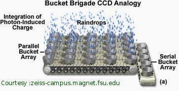 |
| Figure 1. Photon collection by photosite and read-out |
The above paragraph would have provided the functioning of light capturing in a superfluous way. Technical details are trimmed to minimum level so as to highlight the principle of light capture. Knowledge on optics and machining is very important to fabricate lenses. The power of DSLR camera hinges on powerful lenses. Good knowledge on micro electronics is absolutely essential to understand the functioning of sensor, read-out amplifier and A-to-D converter. To design and fabricate reasonable good resolution acquiring subsystem, a sound knowledge on Very Large Scale Integration (VLSI) and knowledge on related software tools are essential. In reality subjects like optics, microelectronics and VLSI are taught even without veiled referenced to camera or scanner systems.
The technology has reached to such a stage that even entry level camera (low priced camera) is capable of taking 10 Mega pixel resolution images. When film based camera reigned, photography was a costly hobby. So very few bought the camera. To acquire digital colour image requires three filters namely red, green, and blue. Use of three filters is costly and instead single sensors are used to cut down the cost. For that 'Bayer Patterns' are used. When Bedaprata Pain [4] and his team developed affordable CMOS active pixel sensor, digital camera become affordable and today every mobile phone is embedded with a camera.
Product Market
The next level of innovation will be in improving usability of camera and not in cost cutting. As the cost comes down heavily quantum of profit will also comes down. To maintain the profit industries go in for volume. Let Camera Company named ABC sells 1000 camera for the price of Rs. 5000. Let the profit be Rs. 500. The net profit is Rs. 5,00,000 (1000 camera x Rs 500). If the same company sells 10000 camera for the price of Rs. 3000 then the net profit is Rs 30,00,000 (10000 camera x Rs 300 as profit). Profit has increased many folds. This logic go well until everyone acquires a camera. After that ABC has find innovative ways to keep the net profit same.
The ultimate aim of the camera manufacturing companies can be put in this way “even a moron should take pictures like a professional photographer.” As we all know we have huge number of amateurs and very few good photographers. The improve the market size of costly DSLR (Digital Single Lens Reflex) camera, industries should target the huge amateur base. But general public neither have patience nor time to become like a professional. To bridge the skill gap lot of intelligence is added in the camera.
Face detection algorithms are used to help to shoot proper pictures by amateurs. Earlier this feature was available in point-and-shoot cameras. Nowadays this feature is extended to professional models like DSLR cameras. Most of us, are unable to set proper ISO, aperture and shutter speed for the required shot. That is why auto-focus and auto-lighting cameras sprung up. But there is a lot scope for improvement in these cameras. Next, amateurs' hands are not stable at the time of taking shot and invariably it results in shaky pictures. This can be corrected by using “image restoration” class of image processing algorithms. Sometimes enough lighting may not be available at the time of shooting or extraneous light may fall on the subject. These errors can be partially corrected using image editing softwares like Photoshop and GIMP. Photoshop is the most popular commercial image editing software and GIMP (GNU Image Manipulation Program) is a open and free software. Lot of image processing algorithms will be deployed in ensuing intelligent camera.
Source
1. How Digital Cameras Work, [Available Online], http://www.astropix.com/HTML/I_ASTROP/HOW.HTM
2. Digital Processing Techniques, [Available Online], http://www.astropix.com/HTML/J_DIGIT/TOC_DIG.HTM
3. ZEISS Microscopy Online Campus | Microscopy Basics | Understanding Digital Imaging, [Available Online], http://zeiss-campus.magnet.fsu.edu/articles/basics/digitalimaging.html
4. Bedabrata Pain - Wikipedia, the free encyclopedia. [Available Online], http://en.wikipedia.org/wiki/Bedabrata_Pain