Wednesday 31 May 2017

Google Lens Technology - Evoked Thoughts

​‌    Sundar Pichai, Chief Executive Officer (CEO) of Google introduced a new technology called Google Lens in the Google IO developer Conference. It was held in the period 17 to 19th of May 2017 at San Francisco, California state, United States of America.  Google IO developer conference is an annual event. It showcases technical in-depth sessions focused on building Web, mobile, and enterprise applications pertaining to Google products and open sources such as Android, Chrome and Chrome OS [1].

      During the demo of Google Lens technology, Mr. Sundar Pichai captured the photo of a flower with a Lens technology enabled Smartphone [2]. The Lens was able to identify the flower. Armed with Lens enabled smart phone, an English man can translate Japanese bill board and understand the content. Take a snapshot of business's storefront and Google Lens will give associated information about the store. In essence Google Lens can understand a picture and act accordingly. Thus Google has provided a new way of interaction with the mobile device. The Google is planning to integrate this technology to Google Assistant. It is expected to be released as an app in upcoming Smartphones. 

Fig. 1. Snapshot of Google Lens enabled Smartphone.  Courtesy [2]

Friday 31 March 2017

Video Quality Vs. Data Rate

       Public are groomed to have insatiable appetite for high resolution,  vivid colour images and videos. This unending desire in one end helps the consumer durable manufacturers to have market for new model televisions and cameras.  In other end the engineers have to burn their mid night oil to find ways and means to solve the challenges posed by high resolution images. 

            Increase in image resolution has a direct bearing on generated volume of data. Few examples are presented to substantiate the claim. Next, reasons for the inability of conventional CMOS interfaces to transport digital data pertaining to high resolution images are discussed.
         

Case I: Digital TV

            In Television (TV) series of frames (images) are shown in succession to create a illusion of motion or continuity. In American system 30 frames are shown per second and European systems use 25 frames per second. In olden day televisions, picture resolution is measured by number of lines and not by number of pixels. They use interlaced scanning with an aspect ratio of 4:3 (Width Vs. Height) is employed. In a digital (Standard Definition or High Definition) TV picture resolution is measured by pixels . Each colour pixel have red, green and blue channel with 8 bit width. So, each colour pixel takes up 24 bits. 

            Net data generated by conventional digital TV titled 480i (suffix i denotes interlaced scanning mode) is
 
480 (V) x 640 (H) x 30 (fps) x 24 (bits) = 0.22 
Gbps (Giga bits per second)             (1)

where V = Resolution in Vertical direction, H= Horizontal direction, fps = frames per second

Tuesday 28 February 2017

OLED - Part II

​‌I. OLED device structure and operation
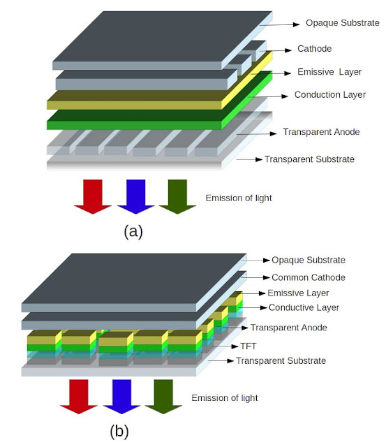
OLED is a multi-layered device. Emissive layer and conductive layer are the most important layers among them. Both layers contain HOMO (Highest Occupied Molecular Orbital) and LUMO (Lowest Unoccupied Molecular Orbital) band. They are analogous to inorganic semiconductors' valence and conduction band.  Emissive layer is connected to cathode and conductive layer is connected to transparent anode. The transparent anode is made up of Indium Tin Oxide (ITO). Electrons are pumped from cathode to emissive layer's LUMO region. Likewise holes are pumped into conductive layer's HOMO region by anode. It reaches emissive layer's HOMO region. As the electron find hole in the emissive layer, it plunges into the hole leaving the excess energy as photon (light particle) [1]. This phenomenon is called electroluminance.  Photon colour depends upon the polymer used in the emissive layer. For example, PPV (polyphenylene vinylene) emits yellow-green light at 510 nm and Poly florene emits blue color. Above the cathode opaque substrate is placed. Below the transparent anode transparent glass is placed. Through the glass generated light passes and reach the viewers. Few more layers are added to improve the efficiency of the OLED. Discussing them is beyond the scope of this article. Human hair is 200 times bigger than OLED structure. So, one can imagine the size of OLED. 

II. OLED Types

OLED can be broadly classified into two categories. One is AMOLED (Active Matrix OLED) and another is PMOLED (Passive Matrix OLED). If faster refresh rates are required as in Television or Smart phone AMOLED is used. Display devices like 16 character display and low end cell phone displays go for PMOLED. As usual they are cheaper to fabricate but their life is limited. PMOLED has stripes of anode and cathode that criss-cross to form a matrix as in Fig 1.(a). In the AMOLED common cathode is used as in Fig. 1. (b). Anode is connected to TFT (Thin Film Transistor) layer. This TFT contains array of Transistors and capacitors. Transistor acts as on-and-off switch and capacitor stores the energy to supply the anode. Refreshing circuitry is used to refresh TFT in regular intervals. Thus each pixel in AMOLED is quickly and accurately energized. Fabrication of TFT into OLED structure is complex but it provides good quality display. Fig 1. (b) is not actual structure. It is author's rendition after studying text related to AMOLED.
It is possible to have transparent cathode instead of transparent anode. Having transparent cathode helps to overcome the restriction posed by TFT structure on the transparent anode. Thus more light is emitted and improvement in pixel brightness and higher resolution is achieved. This  technique is called top emission adaptive current drive technology [1].  
Fig 1. (a) Structure of PMOLED (b) Structure of AMOLED (author's rendition)

Tuesday 31 January 2017

OLED - Part 1

     Present day smart phone display screens are almost made up of OLED (Organic Light Emitting Diode).  Television screens that uses OLED are also available. Due to their high cost it is not ubiquitous in the TV market. OLED emerges as the promising display technology of near future.

Introduction to LED
    Diode is an electronic device. Electronics is a branch of science that deals with study of flow of electrons in a semiconductor or vacuum or gas. Semi is a Latin prefix meaning 'half'. Group 4 elements like Silicon and Germanium has four electrons in the outer orbit and they behave as a perfect semiconductor. Diode is a two terminal device. When current passes through typical diode, small amount heat or infra red emissions occur. But in the case of Light Emitting Diode (LED) instead of heat, light is produced. At present organic materials like polymers are used to make LED. 

Figure 1. (a) Typical LED (inorganic) (b) Symbol for diode (c) Symbol for LED   Image Courtesy: Wikipedia
Organic Polymers
    General public associate the word “Organic” with a produce that is free  from artificial chemicals. In science the word organic is associated with carbon compounds like carbonates, oxides, hydrocarbons and so on.
    Polymers are made up of long chains of molecules. Almost all polymers are organic in nature. Few Inorganic polymers also do exist. Silicone is a best example for inorganic polymer.